- 您现在的位置:买卖IC网 > Sheet目录2011 > MAX5878EGK+D (Maxim Integrated Products)IC DAC 16BIT DUAL 250MSPS 68-QFN
MAX5878
16-Bit, 250Msps, High-Dynamic-Performance,
Dual DAC with LVDS Inputs
4
_______________________________________________________________________________________
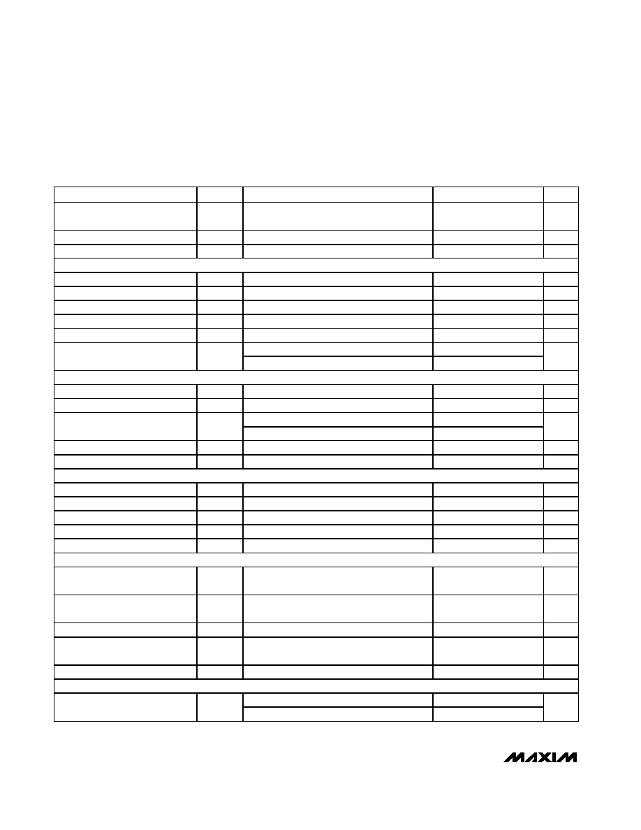
ELECTRICAL CHARACTERISTICS (continued)
(AVDD3.3 = DVDD3.3 = AVCLK = +3.3V, AVDD1.8 = DVDD1.8 = +1.8V, GND = 0, fCLK = 2 x fDAC, external reference VREFIO = +1.25V, out-
put load 50
double-terminated, transformer-coupled output, IOUTFS = 20mA, TA = TMIN to TMAX, unless otherwise noted. Typical values
are at TA = +25°C.) (Note 2)
PARAMETER
SYMBOL
CONDITIONS
MIN
TYP
MAX
UNITS
Reference Input Compliance
Range
VREFIOCR
0.125
1.260
V
Reference Input Resistance
RREFIO
10
k
Reference Voltage Drift
TCOREF
±25
ppm/
°C
ANALOG OUTPUT TIMING (See Figure 4)
Output Fall Time
tFALL
90% to 10% (Note 5)
0.7
ns
Output Rise Time
tRISE
10% to 90% (Note 5)
0.7
ns
Output-Voltage Settling Time
tSETTLE
Output settles to 0.025% FS (Note 5)
14
ns
Output Propagation Delay
tPD
Excluding data latency (Note 5)
1.1
ns
Glitch Impulse
Measured differentially
1
pVs
IOUTFS = 2mA
30
Output Noise
nOUT
IOUTFS = 20mA
30
pA/
√Hz
TIMING CHARACTERISTICS
Data to Clock Setup Time
tSETUP
Referenced to rising edge of clock (Note 6)
-1.2
ns
Data to Clock Hold Time
tHOLD
Referenced to rising edge of clock (Note 6)
2.0
ns
Latency to I output
9
Data Latency
Latency to Q output
8
Clock
Cycles
Minimum Clock Pulse-Width High
tCH
CLKP, CLKN
0.9
ns
Minimum Clock Pulse-Width Low
tCL
CLKP, CLKN
0.9
ns
LVDS LOGIC INPUTS (B15P/B15N–B0P/B0N, XORN, XORP, SELIQN, SELIQP)
Differential Input-Logic High
VIH
100
mV
Differential Input-Logic Low
VIL
-100
mV
Common-Mode Voltage Range
VCMR
1.125
1.375
V
Differential Input Resistance
RIN
(Note 7)
110
Input Capacitance
CIN
2.5
pF
CMOS LOGIC INPUTS (PD, TORB)
Input-Logic High
VIH
0.7 x
DVDD3.3
V
Input-Logic Low
VIL
0.3 x
DVDD3.3
V
Input Leakage Current
IIN
-20
1
+20
A
PD, TORB Internal Pulldown
Resistance
VPD = VTORB = 3.3V
1.5
M
Input Capacitance
CIN
2.5
pF
CLOCK INPUTS (CLKP, CLKN)
Sine wave
> 1.5
Differential Input
Voltage Swing
Square wave
> 0.5
VP-P
发布紧急采购,3分钟左右您将得到回复。
相关PDF资料
MAX5884EGM+D
IC DAC 14BIT 3.3V 200MSPS 48-QFN
MAX5885EGM+D
IC DAC 16BIT 3.3V 200MSPS 48-QFN
MAX5886EGK+D
IC DAC 12BIT 3.3V 500MSPS 68-QFN
MAX5887EGK+D
IC DAC 14BIT 3.3V 500MSPS 68-QFN
MAX5888EGK+D
IC DAC 16BIT 3.3V 500MSPS 68-QFN
MAX5889EGK+D
IC DAC 12BIT LVDS 600MSPS 68-QFN
MAX5890EGK+D
IC DAC 14BIT LVDS 600MSPS 68-QFN
MAX5891EGK+D
IC DAC 16BIT LVDS 600MSPS 68-QFN
相关代理商/技术参数
MAX5878EGK+TD
功能描述:数模转换器- DAC 16-Bit 2Ch 250Msps DAC RoHS:否 制造商:Texas Instruments 转换器数量:1 DAC 输出端数量:1 转换速率:2 MSPs 分辨率:16 bit 接口类型:QSPI, SPI, Serial (3-Wire, Microwire) 稳定时间:1 us 最大工作温度:+ 85 C 安装风格:SMD/SMT 封装 / 箱体:SOIC-14 封装:Tube
MAX5878EGK-D
功能描述:数模转换器- DAC RoHS:否 制造商:Texas Instruments 转换器数量:1 DAC 输出端数量:1 转换速率:2 MSPs 分辨率:16 bit 接口类型:QSPI, SPI, Serial (3-Wire, Microwire) 稳定时间:1 us 最大工作温度:+ 85 C 安装风格:SMD/SMT 封装 / 箱体:SOIC-14 封装:Tube
MAX5878EGK-TD
功能描述:数模转换器- DAC RoHS:否 制造商:Texas Instruments 转换器数量:1 DAC 输出端数量:1 转换速率:2 MSPs 分辨率:16 bit 接口类型:QSPI, SPI, Serial (3-Wire, Microwire) 稳定时间:1 us 最大工作温度:+ 85 C 安装风格:SMD/SMT 封装 / 箱体:SOIC-14 封装:Tube
MAX5878EVKIT
功能描述:数模转换器- DAC Evaluation Kit for the MAX5876/MAX5877/MAX5878 RoHS:否 制造商:Texas Instruments 转换器数量:1 DAC 输出端数量:1 转换速率:2 MSPs 分辨率:16 bit 接口类型:QSPI, SPI, Serial (3-Wire, Microwire) 稳定时间:1 us 最大工作温度:+ 85 C 安装风格:SMD/SMT 封装 / 箱体:SOIC-14 封装:Tube
MAX5878EVKIT#
功能描述:数模转换器- DAC Evaluation Kit for the MAX5876/MAX5877/MAX5878 RoHS:否 制造商:Texas Instruments 转换器数量:1 DAC 输出端数量:1 转换速率:2 MSPs 分辨率:16 bit 接口类型:QSPI, SPI, Serial (3-Wire, Microwire) 稳定时间:1 us 最大工作温度:+ 85 C 安装风格:SMD/SMT 封装 / 箱体:SOIC-14 封装:Tube
MAX5879EVKIT#
制造商:Maxim Integrated Products 功能描述:EVALUATION KIT FOR THE MAX5879 - Boxed Product (Development Kits)
MAX5879EXF+
制造商:Maxim Integrated Products 功能描述:14-BIT, 2.3GSPS DIRECT RF SYNTHESIS DAC WITH SELECTABLE FREQ - Rail/Tube
MAX5879ZEXF+
制造商:Maxim Integrated Products 功能描述:14-BIT, 2.3GSPS DIRECT RF SYNTHESIS DAC WITH SELECTABLE FREQ - Rail/Tube